
Advanced Spectroscopy
|
Nanoscale Characterization and High-Performance Optics


Horiba Spectroscopy
The Spectroscopy portfolio offers a comprehensive suite of analytical instruments designed to characterize materials across electronic, vibrational, and elemental domains, transcending the limitations of conventional bulk analysis. These technologies, ranging from high-resolution chemical imaging via Raman and AFM-Raman to electronic structure determination using Photoluminescence and Cathodoluminescence, provide the site-specific insight necessary to understand complex material function and failure points.
These systems directly address the technological imperative for deeper material insight by offering specialized modes that enhance sensitivity and spatial resolution. Techniques such as Fluorescence Spectroscopy and Time-Resolved Photoluminescence enable the study of molecular dynamics and carrier lifetimes, moving beyond static compositional measurements. Furthermore, the integration of Spectroscopic Ellipsometry provides non-destructive thickness and optical property metrology for multilayer films in semiconductor fabrication, while X-ray Fluorescence Spectroscopy (XRF) offers rapid, non-destructive elemental analysis, collectively ensuring complete material characterization across multiple analytical vectors.
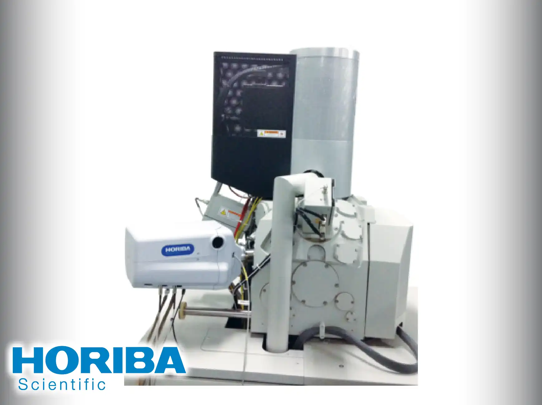
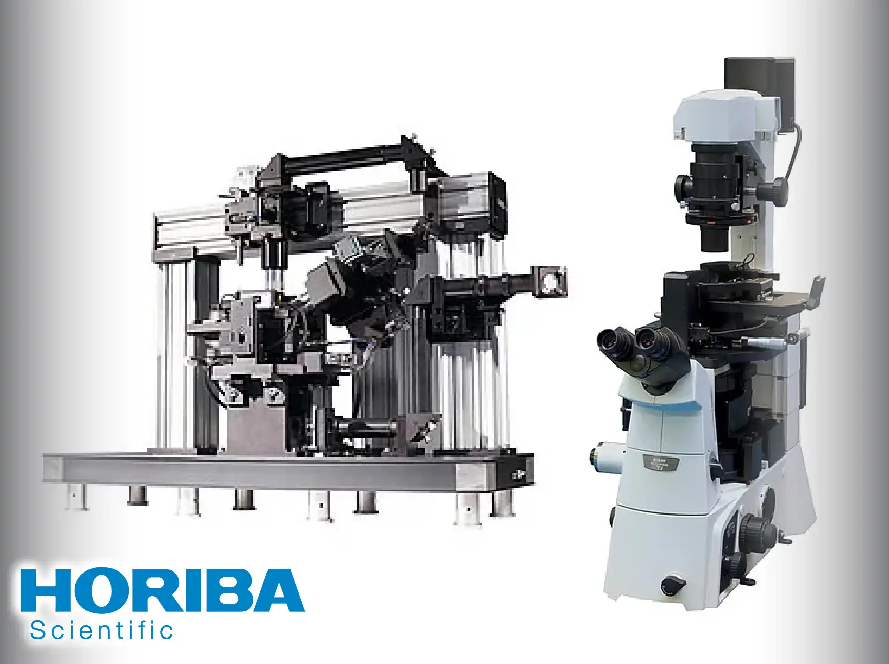
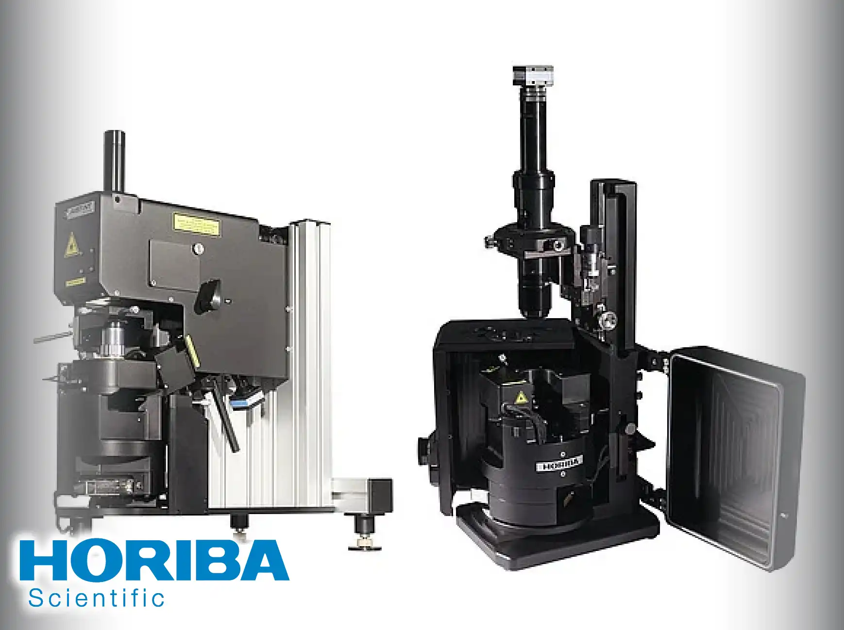
Cathodoluminescence (CL)
CL uses a high-energy electron beam to excite materials, breaking the diffraction limit of light to map electronic properties and defects at sub-100 nanometer resolution. Integrated into Scanning Electron Microscopes (SEM), it correlates surface topography with optical emission, making it vital for diagnosing performance variations in semiconductors and microelectronics.
Raman Spectroscopy
Raman Spectroscopy provides a molecular "vibrational fingerprint" through inelastic light scattering. It identifies chemical structures and phases non-destructively. By measuring small shifts in light (cm−1), it quantifies intrinsic stress and strain in crystalline materials, ensuring structural integrity in engineered components.
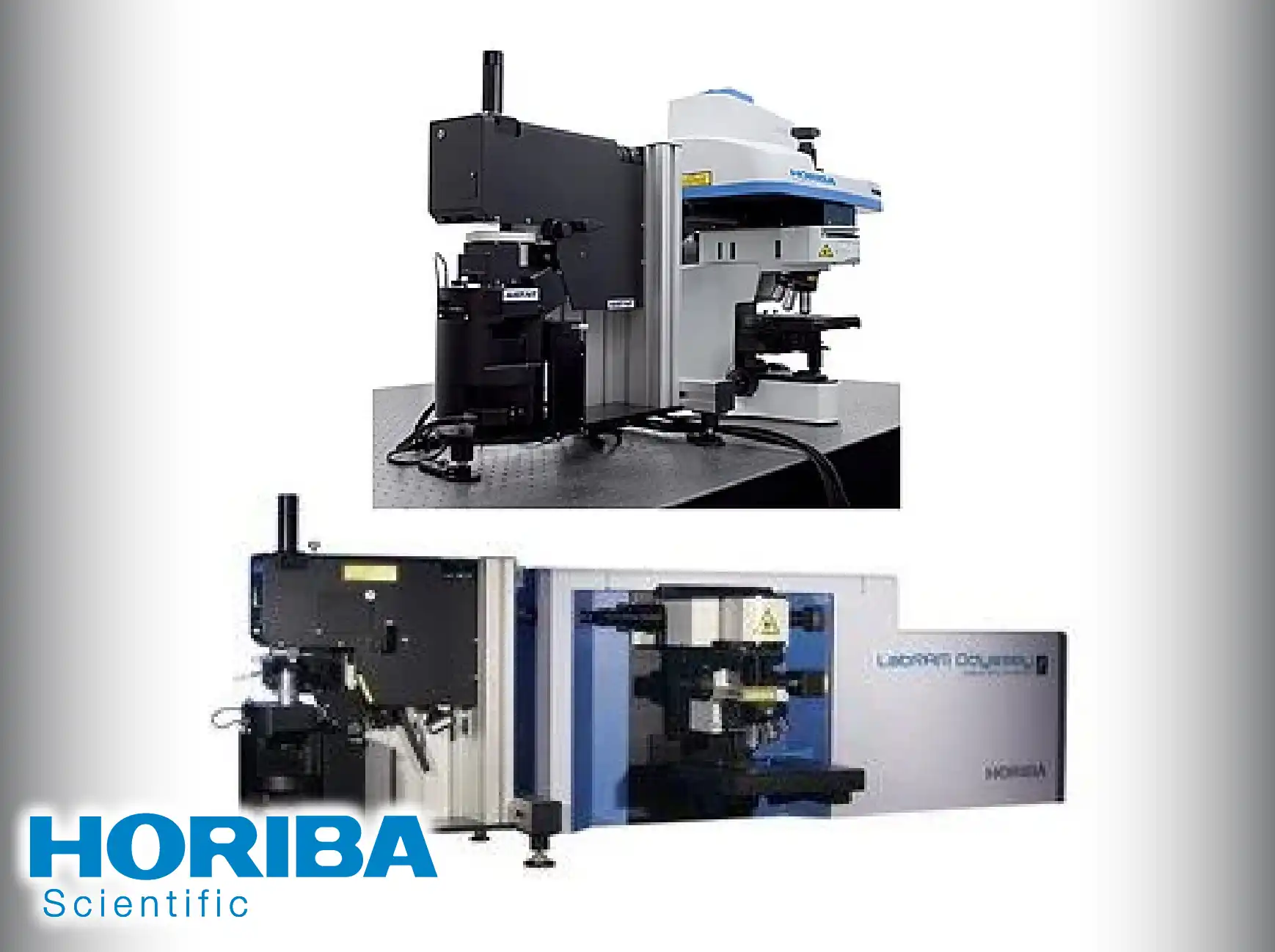
AFM-Raman Integration
This platform combines Atomic Force Microscopy (AFM) with Raman to colocalize physical topography and chemical composition at the same point. It enables Tip-Enhanced Raman Spectroscopy (TERS), which uses a plasmonic tip to achieve chemical mapping at the nanometer scale, far surpassing the limits of standard optical microscopy.
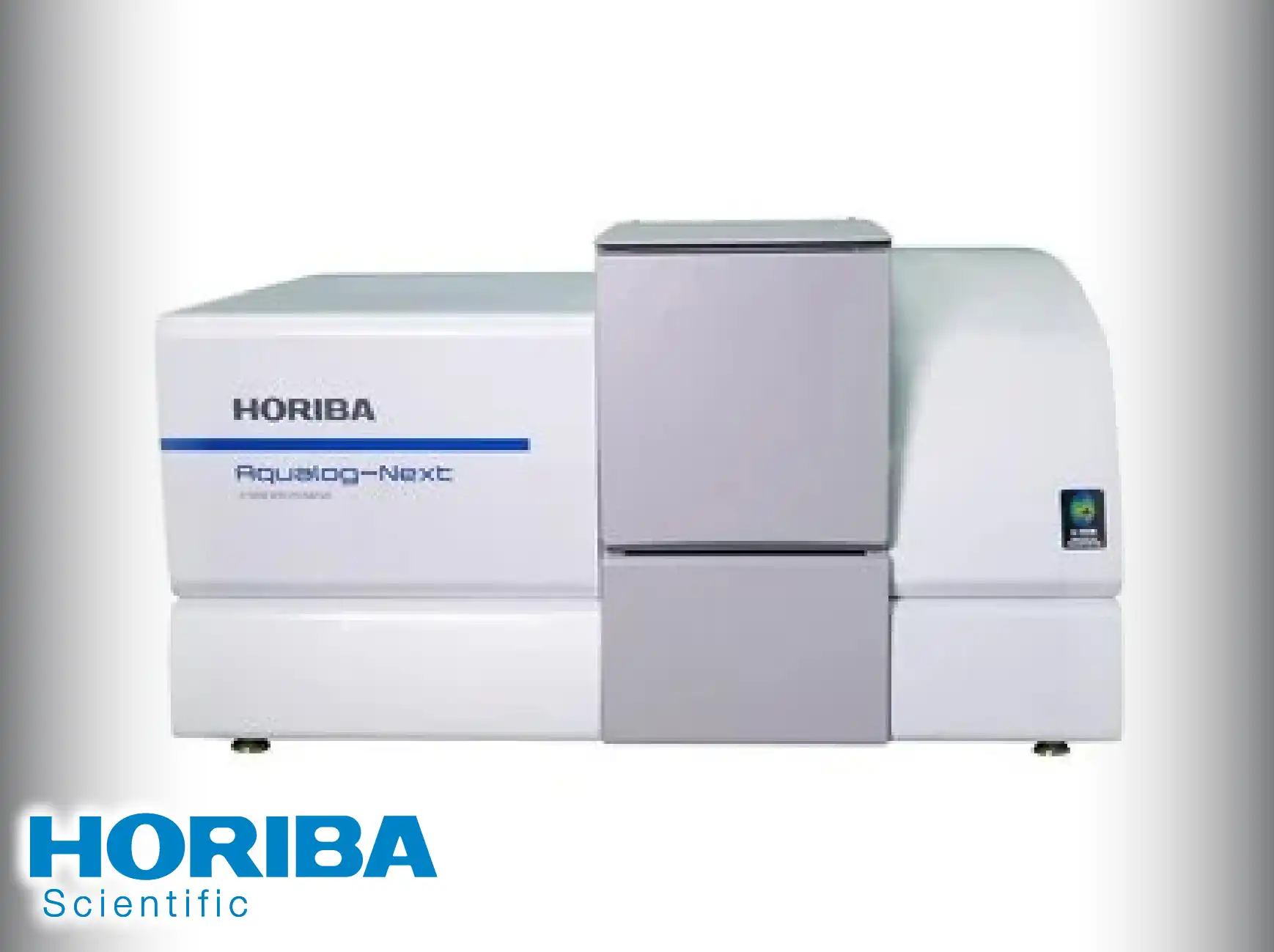
Fluorescence & Photoluminescence (FS/PL)
Fluorescence (FS) and Photoluminescence (PL) probe electronic states by measuring emitted light following photon absorption. While FS is a cornerstone for bioanalysis using molecular tags, PL is essential for determining the band gap and carrier lifetimes in semiconductors, which are critical metrics for solar cell and LED efficiency.
Spectroscopic Ellipsometry (SE)
SE is a precise optical metrology technique that measures the change in light polarization upon reflection. It is used to determine the thickness and optical constants (refractive index and absorption) of thin film stacks. Its non-destructive nature and nanometric sensitivity make it a standard in semiconductor manufacturing.
Core Components: Detectors & Gratings
Instruments rely on specialized detectors (CCDs, PMTs, InGaAs) and diffraction gratings to capture and disperse light. Deep cooling reduces thermal noise, while high-density gratings ensure spectral resolution. These components are optimized to convert individual photons into accurate data across the UV, Visible, and NIR spectrums.
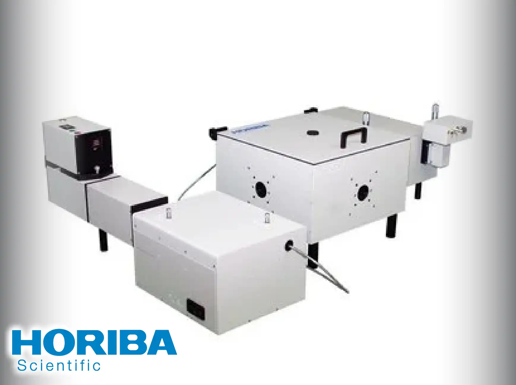
Monochromators & Spectrographs
These units isolate specific wavelengths of light. Monochromators use scanning mechanisms for high-accuracy single-wavelength analysis, while spectrographs utilize array detectors to capture an entire spectral range simultaneously. Their focal length and mechanical stability directly dictate the system's ultimate resolution.
X-ray Fluorescence Spectroscopy (XRF)
XRF provides non-destructive elemental analysis by exciting a sample with X-rays and measuring the resulting characteristic fluorescent emission. It identifies elements from Beryllium to Uranium and is widely used for rapid quality control, allowing for quantification of elemental concentrations from 100% down to sub-ppm levels.
Click here for more information about Horiba Solutions